- 您现在的位置:买卖IC网 > Sheet目录1990 > CDCR83DBQG4 (Texas Instruments)IC DIRECT RAMBUS CLK GEN 24-QSOP
CDCR83
DIRECT RAMBUS CLOCK GENERATOR
SCAS632B APRIL 2001 REVISED OCTOBER 2005
7
POST OFFICE BOX 655303
DALLAS, TEXAS 75265
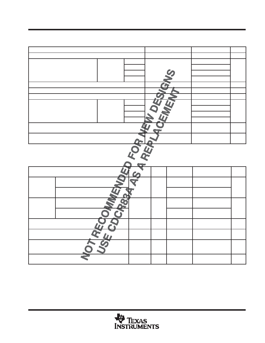
switching characteristics over recommended operating free-air temperature range (unless
otherwise noted)
PARAMETER
TEST CONDITIONS
MIN
TYP
MAX
UNIT
tc(out)
Clock output cycle time
2.5
3.75
ns
Total cycle jitter over 1, 2,
Infinite and
267 MHz
80
t(jitter)
Total cycle jitter over 1, 2,
3, 4, 5, or 6 clock cycles
Infinite and
stopped phase
300 MHz
See Figure 3
70
ps
t(jitter)
3, 4, 5, or 6 clock cycles
stopped phase
alignment
356 MHz
See Figure 3
60
ps
alignment
400 MHz
50
t(phase)
Phase detector phase error for distributed loop
Static phase error}
100
ps
t(phase, SSC)
PLL output phase error when tracking SSC
Dynamic phase error}
100
ps
t(DC)
Output duty cycle over 10,000 cycles
See Figure 4
45%
55%
Infinite and
267 MHz
80
t(DC, err)
Output cycle-to-cycle
Infinite and
stopped phase
300 MHz
See Figure 5
70
ps
t(DC, err)
Output cycle-to-cycle
duty cycle error
stopped phase
alignment
356 MHz
See Figure 5
60
ps
duty cycle error
alignment
400 MHz
50
tr, tf
Output rise and fall times (measured at 20%80% of
output voltage)
See Figure 7
160
400
ps
t
Difference between rise and fall times on a single device
(20%80%) |tf tr|
See Figure 7
100
ps
All typical values are at VDD = 3.3 V, TA = 25°C.
Assured by design
state transition latency specifications
PARAMETER
FROM
TO
TEST
CONDITIONS
MIN
TYP
MAX
UNIT
t(powerup)
Delay time, PWRDNB
↑ to CLK/CLKB output
settled (excluding t(DISTLOCK))
Powerdown
Normal
See Figure 8
3
ms
t(powerup)
Delay time, PWRDNB
↑ to internal PLL and
clock are on and settled
Powerdown
Normal
3
ms
t(VDDpowerup)
Delay time, power up to CLK/CLKB output
settled
VDD
Normal
See Figure 8
3
ms
t(VDDpowerup)
Delay time, power up to internal PLL and
clock are on and settled
VDD
Normal
3
ms
t(MULT)
MULT0 and MULT1 change to CLK/CLKB
output resettled (excluding t(DISTLOCK))
Normal
See Figure 9
1
ms
t(CLKON)
STOPB
↑ to CLK/CLKB glitch-free clock
edges
CLK Stop
Normal
See Figure 10
10
ns
t(CLKSETL)
STOPB
↑ to CLK/CLKB output settled to
within 50 ps of the phase before STOPB was
disabled
CLK Stop
Normal
See Figure 10
20
cycles
t(CLKOFF)
STOPB
↓ to CLK/CLKB output disabled
Normal
CLK
Stop
See Figure 10
5
ns
All typical values are at VDD = 3.3 V, TA = 25°C.
发布紧急采购,3分钟左右您将得到回复。
相关PDF资料
CDP68HC68T1M
IC RTC 32X8 NVSRAM CMOS 20-SOIC
CPLL66-1600-2200
IC VCO PLL/SYNTH 2.2GHZ SMD
CPLL66-2175-2175
IC VCO PLL/SYNTH 2175MHZ SMD
CPLL66-2400-2500
IC VCO PLL/SYNTH 2500MHZ SMD
CPLL66-2450-2450
IC VCO PLL/SYNTH 2450MHZ SMD
CPLL66-3160-3380
IC VCO PLL/SYNTH 3380MHZ SMD
CPLL66-3475-3475
IC VCO PLL/SYNTH 3475MHZ SMD
CPLL66-4160-4380
IC VCO PLL/SYNTH 4380MHZ SMD
相关代理商/技术参数
CDCR83DBQR
功能描述:时钟发生器及支持产品 400MHz Direct Rambus (TM) Clock Gen RoHS:否 制造商:Silicon Labs 类型:Clock Generators 最大输入频率:14.318 MHz 最大输出频率:166 MHz 输出端数量:16 占空比 - 最大:55 % 工作电源电压:3.3 V 工作电源电流:1 mA 最大工作温度:+ 85 C 安装风格:SMD/SMT 封装 / 箱体:QFN-56
CDCR83DBQRG4
功能描述:时钟发生器及支持产品 400MHz Direct Rambus (TM) Clock Gen RoHS:否 制造商:Silicon Labs 类型:Clock Generators 最大输入频率:14.318 MHz 最大输出频率:166 MHz 输出端数量:16 占空比 - 最大:55 % 工作电源电压:3.3 V 工作电源电流:1 mA 最大工作温度:+ 85 C 安装风格:SMD/SMT 封装 / 箱体:QFN-56
CDCS501
制造商:TI 制造商全称:Texas Instruments 功能描述:SSC Clock Generator/Buffer
CDCS501PW
功能描述:时钟发生器及支持产品 Clock Driver w/ Opt Spread-Spect Clock RoHS:否 制造商:Silicon Labs 类型:Clock Generators 最大输入频率:14.318 MHz 最大输出频率:166 MHz 输出端数量:16 占空比 - 最大:55 % 工作电源电压:3.3 V 工作电源电流:1 mA 最大工作温度:+ 85 C 安装风格:SMD/SMT 封装 / 箱体:QFN-56
CDCS501PW
制造商:Texas Instruments 功能描述:Clock IC
CDCS501PWR
功能描述:时钟发生器及支持产品 Clock Driver w/ Opt Spread-Spect Clock RoHS:否 制造商:Silicon Labs 类型:Clock Generators 最大输入频率:14.318 MHz 最大输出频率:166 MHz 输出端数量:16 占空比 - 最大:55 % 工作电源电压:3.3 V 工作电源电流:1 mA 最大工作温度:+ 85 C 安装风格:SMD/SMT 封装 / 箱体:QFN-56
CDCS502
制造商:TI 制造商全称:Texas Instruments 功能描述:Crystal Oscillator / Clock Generator with optional SSC
CDCS502_12
制造商:TI 制造商全称:Texas Instruments 功能描述:Crystal Oscillator / Clock Generator with optional SSC